The Reclone Rise will be a friendly and flexible reconfigurable computing platform geared towards education and enthusiasts. Its design will be completely open-source, along with a support forum, readthedocs, and SDK. Initial prototypes will be designed and assembled in the USA.
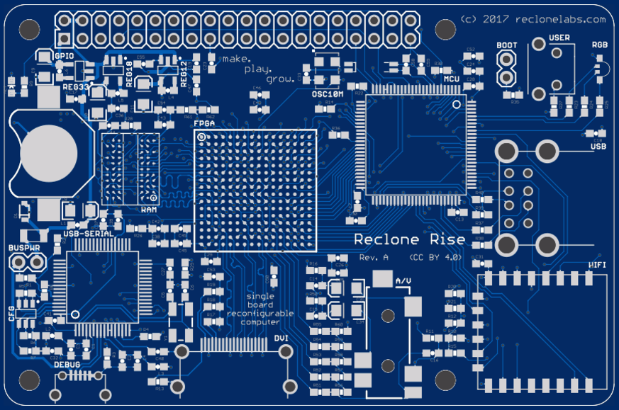
Reclone Rise rev A, top side. Almost all surface-mount components are placed on the top to make it easier to reflow solder later.
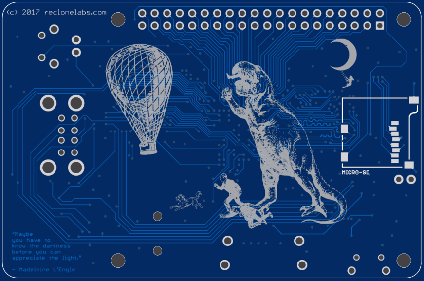
Reclone Rise rev A, bottom side. The designer had some fun with openclipart.org and a somewhat odd quote.
Perspective
This is NOT just another open-source board with a chip, a power supply, a bunch of pins, and the hope of community support. Nor is it an expensive commercial evaluation board meant to advertise the capabilities of one specific chip.
The Rise is meant to demonstrate that an integrated MCU+FPGA solution is more powerful, flexible, and easy to use than the sum of its parts. It will prove that you can accomplish many of the capabilities of a single-board computer at quicker latencies, lower clock speeds, and lower power consumption. It will make FPGA SoC development much easier, with the “hard stuff” like network communication, file system, and USB host offloaded to a dedicated microcontroller. It will unlock new capabilities for microcontroller development, including easy audio and video output, megabytes of available RAM, and a fabric for running accelerator cores to speed up specific applications.
For educators, one flexible hardware platform can serve the needs of an entire computer engineering or embedded systems curriculum. Or, it can introduce students to programming, while using modern debugging techniques and bypassing the traditional Linux learning curve. Reclone Labs is dedicated to the promotion of STEM education and is willing to work to support educators by creating written lab materials and online coursework.
For students of all levels, the Rise can be programmed in quite a few high-level languages (Python, Lua, Scheme, Arduino/C/C++, JavaScript, and Rust, to name a few). Then, discover several real-time operating systems (NuttX, FreeRTOS, ChibiOS, mbed OS), try on embedded Linux for size (uClinux), or program on “bare metal”. Finally, dive into the finer points of computer architecture by learning assembly language, VHDL, and Verilog, and design your own processor or SoC.
For makers, hobbyists, and prototypers, the Rise is mechanically- and expansion header-compatible with the Raspberry Pi 2 and 3 Model B. Consider porting your Raspberry Pi or Arduino project to the Rise for more integrated capabilities, better real-time performance, or lower power consumption. Furthermore, the FPGA, MCU, and WiFi module on the Rise are commercially available in low quantities, and already have extensive community support. Reclone has made its Eagle design files open source, so you are free to spin your own board designs based on the Rise (with attribution, please).
For retro computing enthusiasts and retro gamers, finally there is a universal platform designed to clone the hardware of those beloved retro systems using modern connectivity, and without the latencies and shortcomings of traditional software-based emulators. Using modern USB mice, keyboards, and gamepads, enjoying those lovely pixelated graphics on your HDTV, and playing retro games online with friends or in a ladder – all of this is possible, in time. Reclone Labs will work to develop this idea as the Rise comes to life.
Specifications
Field Programmable Gate Array (FPGA)
- Xilinx Spartan-6 XC6SLX16FTG256
- 2278 slices; 18224 flip-flops; 32 DSP slices; 136 Kb Distributed RAM; 576 Kb Block RAM; 2 clock management tiles
- 1.2V core voltage; 1.8V and 3.3V I/O bank voltage standards
- FPGA (re-)configuration occurs at runtime via MCU Slave Serial interface
- Xilinx ISE WebPack: Free (no cost) design suite and toolchain
Microcontroller (MCU)
- STMicroelectronics STM32F405VGT6
- ARM Cortex-M4 32-bit microcontroller with FPU
- System clock up to 168 MHz
- 1 MByte Flash, 196 KBytes total internal SRAM
- SDIO, USB, SPI, Analog, PWM, UART, DMA, and other peripherals
- Connected to FPGA via Flexible Static Memory Controller (FSMC) bus interface for memory-mapped soft cores or additional RAM
- Several free and low-cost toolchain and IDE choices, including GNU MCU Eclipse, CooCox, and Code::Blocks
WiFi
- Pine64 PADI module with Realtek RTL8710AF
- FCC/CE certified 802.11 b/g/n
- Interfaces: 4-bit SDIO, UART, JTAG
RAM
- 64Mx8 bit DDR2 SDRAM @ 1.8V
- Burst transfer rates up to 800 MByte/sec @ up to 400 MHz clock
- Connected to hard memory controller in FPGA
USB Host
- Two onboard USB-A ports
- Dual USB 2.0 Full-speed host peripherals on MCU
Power
- Micro USB port provides 5V source (from PC, TV, cell phone charger, etc.)
- Removable “Bus Power” jumper allows connection of +5V from an external source, addition of power switch or battery circuit, easy current measurement, etc.
- Many applications can run on less than 500mA (2.5W)
Debugger & Console
- Onboard debugger: FT2232H USB 2.0 to serial chip on micro USB port
- JTAG Interface: connected to MCU, WiFi module, and FPGA in a JTAG chain for in-circuit programming, debugging, and boundary scan
- UART Interface: connected to MCU for console, logging, or brick-busting
Audio/Video
- HDMI port: TMDS interface via FPGA; video output at 720p60, 1080i60, or 1080p30; digital audio output capable (not planned or intended to be fully HDMI certified or compliant)
- Analog A/V jack: 4-conductor 3.5mm stereo line-out and composite video output (Pi compatible)
Micro SD
- Onboard holder accepts standard microSD and microSDHC cards
- File system: FAT or FAT32 (possibly others; depends on application/drivers)
- A microSD card is not required by many applications (MCU has internal program/data Flash, unlike the Raspberry Pi)
Expansion Header
- 2×20 pin male header
- 28 pins connected to 3.3V LVTTL I/O on FPGA
- Electrically and physically compatible with accessories designed for the Raspberry Pi
- Two 0-3.3V analog input pins connected to MCU (pins chosen for compatibility with mikroBUS Pi 2 click shield)
Extras
- Real-time clock: 12mm coin cell; 32.768 kHz crystal; backup registers and SRAM available in MCU
- User button: connected to microcontroller’s WAKE input
- Tri-color RGB LED: for vibrant application-specific indication
Current Status
One prototype has been partially hand-soldered, excluding the FPGA, RAM, HDMI, and A/V, with the goal of incrementally bringing up NuttX configuration and driver support.
This is what works so far:
- NuttX
- A Reclone fork of the main NuttX repository has been established.
- Board support has been added as “reclone-rise”.
- 10MHz Oscillator module
- Support for external oscillator clocking has been coded and contributed back to the NuttX mainline.
- Through the HSE PLL, MCU runs stable at its maximum 168 MHz system clock.
- Real-time Clock (RTC)
- Using HSE as a timing source. (32.768 kHz RTC crystal clock source is NOT working – I suspect a soldering issue.)
- RTC support has been enabled and tested in NuttX.
- Verified that CR1216 3V battery maintains backup registers.
- RGB LED
- Produces bright and beautiful colors.
- Support for common-anode RGB LEDs and approximate CIE 1931 lightness correction for good color blending has been coded and contributed back to the NuttX mainline.
- FT2232H
- USB-to-JTAG: OpenOCD detects and flashes the MCU successfully. (added bodge wires to complete JTAG chain in the absence of WiFi and FPGA)
- USB-to-UART: PuTTY connects to the Nuttx NuttShell; verified that ST’s “Flash Loader Demonstrator” can be used to brick-bust the MCU using its system boot loader.
Some of the errata found and lessons learned, which should lead to improvements in Rise rev B:
- Use the Pine64 PADI instead of ESP-12F. The PADI is ARM Cortex-M3-based, has better JTAG support, can use program flash and SDIO at the same time, and therefore can be programmed as a FullMAC SDIO WiFi device for use with NuttX.
- Re-arrange the right side of the board to keep the whole WiFi module (including antenna) within board outline, so that nothing has to protrude out of a case. Probably the USB ports will be moved to the top, and the LED and button moved to the upper middle, to make room for the PADI.
- Pick different 1.8V switching regulator, as this one has problematic soft start behavior. Sometimes I need to re-plug the board a few times to get the 1.8V rail to come up and power the FT2232 chip.
- Tweak tStop and bStop layers to provide a translucent window in the board to let the LED shine through, and to widen the mounting hole area
- Need to select some substitute parts for easier hand soldering and to solve obsolescence issues.
Another, more complete, prototype including the BGA components will be either professionally assembled or “cooked” in a toaster oven.


Hi Jeff,
I’m looking forward for news!
Please keep us updated! 😉